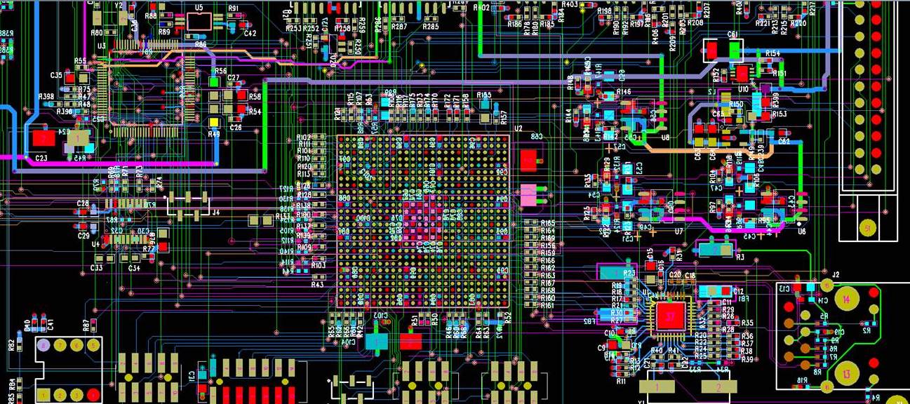
Case study: 8 and 14-layer HDI with Stacked Vias
4.7 (537) · $ 26.00 · In stock

This case study focuses on the challenges and solutions that we implemented to design complex HDI boards with stacked vias.
14 Layer PCB HDI Vias in Pad BGA

An in-depth analysis on PCB stackup – PCB HERO

How to Plan Multilayer PCB Stackup - RAYPCB

HDI PCB Stackup - Venture Elctronics

Understanding Proper PCB Design (Part 2) - Circuit Cellar

Stacked and Staggered Via to Optimize PCB Design and Manufacturing
The impact of HDI and microvias on PCB design - Tech Design Forum Techniques
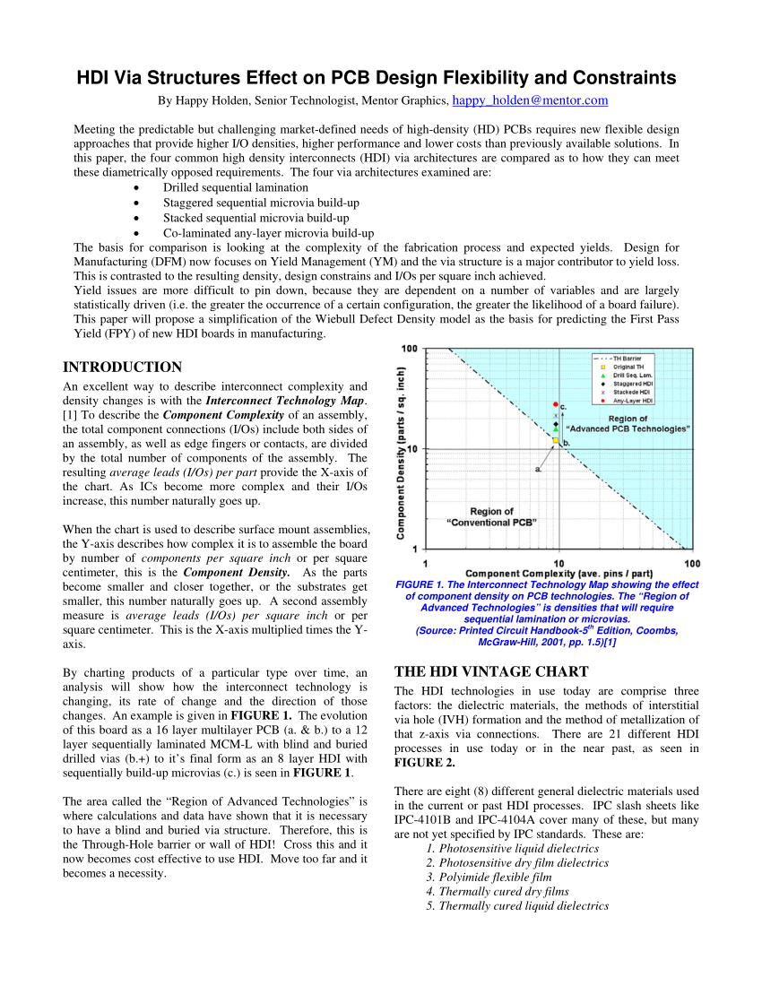
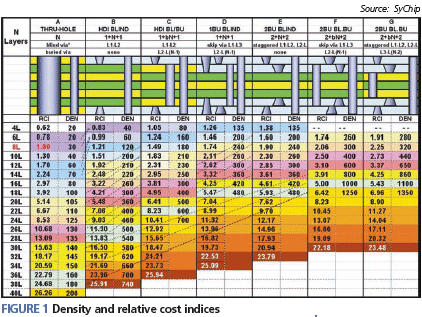
PDF) HDI via structures effect on PCB design flexibility, constraints and cost

HDI PCB Stackup - Venture Elctronics

How to Design Your HDI PCB Stackup
Your Guide to Flexible PCB Design & Layout

Explain Like I'm a Designer: ELIC PCB and HDI Routing, HDI Design